Notes of IIIS Computer Architecture course, Spring 2022, taught by Prof. Mingyu Gao.
01: basic concepts
Von Neumann Architecture: separate processor/memory
Code Compilation & Translation: High-level(*.c) -> Assembly(*.s) -> Machine object(*.o) -> executable
Processors: realizes ISA (RISC vs CISC)
Registers
Memory: Byte-Oriented Memory Accessing
- Big-endian & little-endian (significant byte -> lower/higher addr.)
Memory mapping: Stack(calling, the bottom has high address), Heap(dynamic data)
02: Metrics
Performance: latency(time for one task) & throughput(# tasks per unit time)
- Performance = (Execution time)$^{-1}$
- Speedup of X over Y = Perf$_X$ / Perf$_Y$.
- Execution time = #Cycles $\times$ CCT(clock cycle time)
Normally, we can use #Cycles to approximate exe. time.
CPI: cycles per instruction
- #Cycles = IC $\times$ CPI, IC = instruction count in one program
-
Execution time = IC $\times$ CPI $\times$ CCT
- Average CPI = $\sum$ IC / IC$_i$ $\times$ CPI$_i$.
Impact of memory, i.e., data accesses, could be reflected on CPI. Roofline model:
Means of metrics: Amean for absolutes; Hmean for rates; Gmean for ratios
Power & energy efficiency
Scaling:
- Strong scaling: speedup on N processors with fixed total workload size
-
Weak scaling: speedup on N processors with fixed per-processor workload size
- Limitation: imbalanced load; Amdhal’s Law: an optimization accelerates a fraction $f$ of a program by a factor of $S$, then speedup = $1/(1-f+f/S)$.
03 RISC-V ISA and Assembly
RISC-V system states: PC, 32 registers x0~x31(alias), memory from 0 to MSIZE-1
Special registers: ra, tp, sp, gp.
Some details:
- 12-bit signed offset in
lwandswinstruction; (most case) - 12-bit immediate in most instructions;
- 20-bit immediate in
luiandauipcfor loading the whole immediate.
04 RISC-V encoding
Six instruction formats:
- R-format: register-register operations
- I-format: register-immediate operations, loads, jalr (12-bit imm, 11:0)
- S-format: stores (12-bit imm, 11:0)
- B-format: branches (12-bit imm, 12:1)
- J-format: jumps (20-bit imm, 20:1)
- U-format: upper immediate instructions (20-bit imm, 31:12)
ISA for parallelism
- SIMD: data-level parallelism
- Example: Intel x86 SSE and AVX Extensions
- SIMD intrinsics: use C functions instead of inline assembly to call SSE/AVX instructions
- MIMD: thread-level parallelism
- process and thread
- Shared-memory multi-core processors
- ISA: Atomic instructions (A extension)
- Another possibility: using locks
05 Decoding & processor
Simple format of RISC-V $\to$ simple instruction decoding
Multi-level decoding:
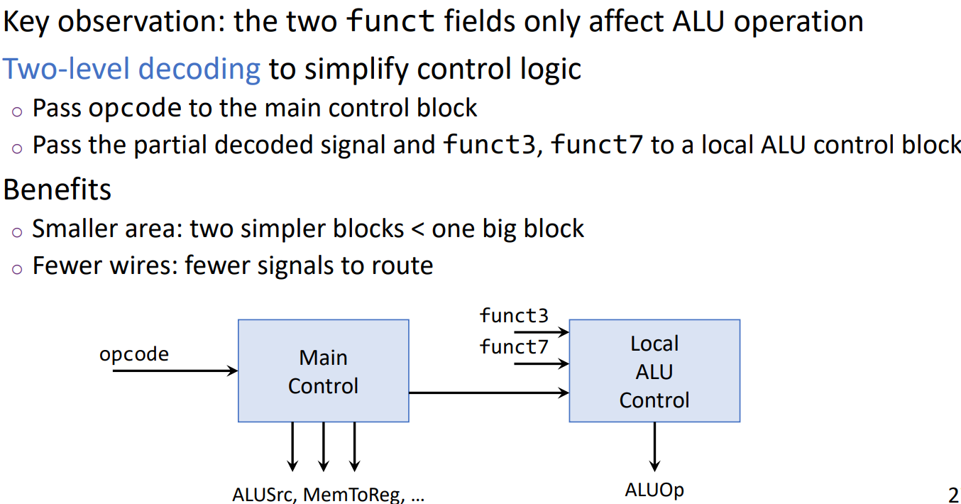
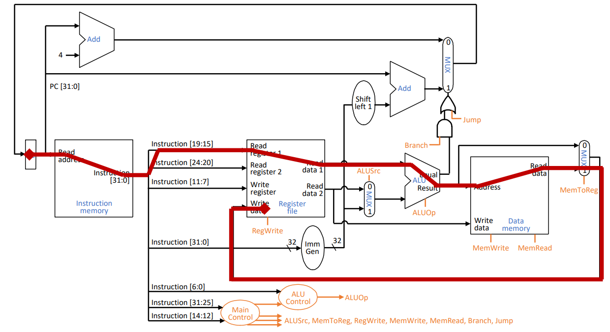
Datapath & control bits
Structure & critical path:
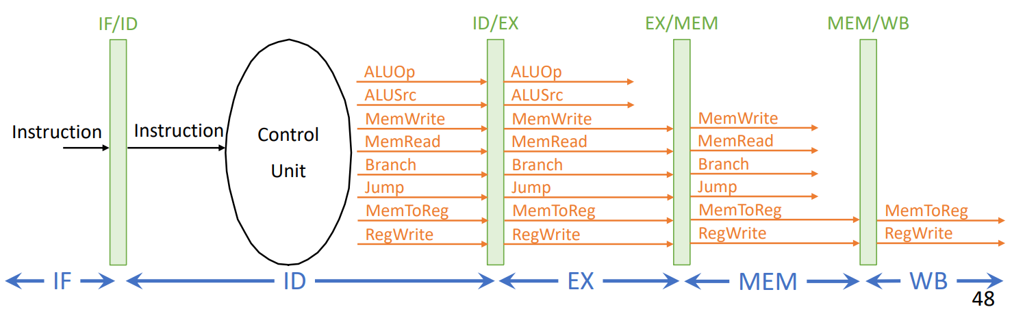
Pipelining: 5 stages IF/ID/EX/MEM/WB
06 Avoiding hazards and stalls
Stalls: a pipeline “bubble”, not moving forward in that cycle
-
How to stall: insert
nopinstructions, or let the hardware stall as needed. -
Causes of stalls: hazards
Hazards:
- Structural hazard: A required resource is busy and cannot be used in this cycle
- different read/write ports; half-cycle register access
- cancel stage bypassing
- seperated memory(IM, DM)
- let multi-stage instructions go
- Data hazard: Must wait previous dependent instructions to produce/consume data (RAW in typical)
- Solution: forwarding
- EX, MEM, WB $\to$ EX, MEM
- forwarding control logic
- exchange the order of instructions to avoid stalls
- Control hazard: Next PC depends on previous instruction
- Resolving branch/jump earlier (in ID stage)
- Furthermore: predict the next PC (usually, PC+4)
- In case of misprediction, we need to nullify the operations and restart as soon as possible.
- Additional forwarding to ID for branches
07 Advanced Techniques
Branch prediction
Key idea of hardware-based prediction: predict based on recent history
Predicting direction:
-
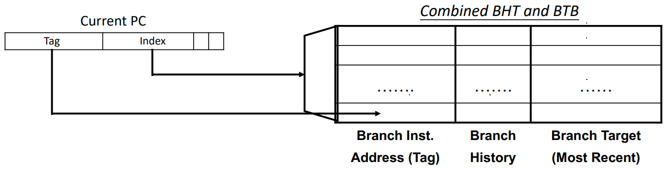
A hardware branch history table (BHT) records each branch’s history
-
Each branch maintains a saturate counter to predict the next direction
- Counter +1 for an actually taken branch, -1 for not-taken
- 1-bit states: 0: predict not-taken, 1: predict taken
- 2-bit states: 00: predict not-taken, 01: not-taken?, 10: taken?, 11: taken
- Simple 2-bit BHT already achieves > 90% accuracy for most programs
Predicting target: Branch target buffer (BTB)
- Record previously executed branches and their most recent target addresses
- Such a hardware table is implemented using SRAM
- Address is branch instruction address, i.e., current PC
- Data is the most recent target, i.e., next PC
Overall workflow
- At IF stage, if BHT predicts to be not taken, then PC = PC + 4
- Else, use current PC to index into BTB
- If there is an entry, then PC = target address in BTB, else PC = PC + 4
Superscalar and Out-of-Order
ILP: Instruction-Level Parallelism = critical path / # instructions
Superscalar execution: multi-instructions per cycle
Out-of-Order (OoO) Execution
- Use diversified functional units to finish instructions ASAP to avoid blocking
- Use inter-stage buffers for decoupling stages and reordering instructions
Stages: Fetch
- decode: also read registers
-
Dispatch/rename/allocation: Resolve dependencies and prepare for OoO execution
- Issue/schedule: Determine whether instruction is ready to execute
- Execute: actual execution of instructions, e.g., ALU, memory access
- Commit/retire/write-back: Update architectural states (registers or memory)
- Each stage can be one or more cycles
08 Cache Design
Idea: Locality (Temporal & Spatial) in programs, both data and instructions; Faster access of a small subset. Cache: Implemented as a processor component (SRAM on chip), managed by hardware, multi-level.
- Miss Handling: Stall the pipeline, fetch (may replace) a block. $\text{CPI penalty = Miss rate} \times \text{Miss penalty}$. $AMAT = \text{Hit latence} + \text{Miss rate} \times \text{Miss penalty}$.
- Organization:
-
Fully-Associative: Tag = block address = Byte Address / Block Size (remove offset bits); high hit latency
-
Directly-mapped: (typical) index = lower bits in block address; high miss rate
-
$N$-way Set-Associative: Each block can go to one of $N$ (Associativity) entries in cache (a set):
\(\text{Set Index} = (\text{Block Address}) \mod (\text{\# Sets in cache}) = \text{Lower bits in block address}.\)
- Extra components: Valid bits, Dirty bits (if necessary), replacement policy.
-
- Physical Organization & accessing
- Tag, index, offset
- Use index bits to locate a set
- For each entry in the set: Check if valid bit is 1, Compare if tag matches.
- If found one such entry, hit, return data, use offset to select bytes in block
- If not found, miss, fetch data from memory, return data, and replace
Types (3C) of misses: Compulsory/cold, Capacity, Conflict
Thrashing: Sequential scanning for multiple times, causing insufficient capacity.
Replacement policies: random, LRU, LFU
- Implementation bits
- Goal: Balady’s optimal: choose the one used again furthest in the future. Match locality charateristics.
Write policies:
- Write through: write in both cache (if exists) and memory. write-alloc vs no-write-alloc.
- Write back: only write in cache; need a dirty bit per block to write back at eviction; fetch if not in cache.
Write buffer: a FIFO buffer between cache and memory; absorb small bursts; might serve for data misses.
Multi-level Caches: AMAT = L1 hit latency $\times$ L1 miss rate $+$ L2 AMAT = $\cdots$.
- Typical Structure: L1-D, L1-I, L2 unified per core, L3 shared last-level, Main memory
- Inclusive vs Exclusive vs Non-inclusive
Private & Shared Caches: Large caches are usually banked; lower hit latency, more parallelism;
Public Cache banking:
- Dynamic block placing: a block is preferred to be placed in the bank closer to the core with the most accesses to it, and may also be migrated between banks; at any time, a block still can only be in one bank; minimize physical distance
Private Cache coherence: a read access should return the most recently written value
- Cache cohenrence protocol: Single-writer, multiple reader (SWMR)
- MSI protocol: [Modified-Shared-Invalid]
- Extend the valid bit to represent 3 states
- Each private cache needs to be told the actions of others
- Snooping: All caches broadcast their misses through the interconnect
- Directory-based: Use a directory to track the state of each block
Non-Blocking Caches: hit-to-miss, hit-under-miss, miss-under-miss Miss status handler register (MSHR): keeps track of outstanding cache misses, pending load & stores refering to that block.
- Fields of an MSHR: Valid bit, block address, multiple pending load/store entries(Valid, type&format, offset, dst/src register)
- Operations
Prefetching: predict and fetch data into cache before processors request it. Reduce cold misses; higher bandwidth consumption; require OoO and non-blocking caches.
- Software prefetch instructions / Hardware prefetchers.
- Stream fetching, Strided fetching(PC-based stride detection)
- Metrics: Accuracy, Coverage, Timeliness
Code-level optimization: loop reordering, loop blocking, false sharing
09 Main memory: DRAM
Hierarchy: CPU - Channel - Rank - Chip - bank
Physical address $\to$ <channel x, rank y, bank z>
- Channels are fully independent, accessed with separate buses
- burst transfer: double-data-rate, transfer on both clk edges.
- NUMA: non-uniform memory access, faster to access local channels.
- Ranks in one channel share I/O, but with independent access
- Each access goes to one rank by “ChipSelect” signal;
- Different ranks in one channel share command/address/data lines (I/O)
- Fully sychronous access across all chips in a rank, providing wide data bus from narrow chip pins
- Chips in one rank share command/address lines, but separate data lines. Fixed granularity.
- Banks in one chip share I/O, but with independent access.
- Banks operate independently, but share command/address/data buses; support concurrent accesses.
DRAM Bank: $2^n$ rows, $2^m$ columns with $2^m \times w$ bitlines, $w$ bits I/O width, $2^m\times w$ bits row buffer Overfetch: accessing one cell must activate the entire row to row buffer. row hit & row miss. Operations: ACTIVATE(open a row), READ, WRITE, PRECHARGE(close the row, clear row buffer), REFRESH
Memory Controller: inside the processor chip, decides address mapping and translate commands, manage row buffer and DRAM refresh.
- DRAM access latency: CPU$\to$memory controller tranfer time, controller latency, DRAM bank latency = $[t(\text{row to column command delay}), t(\text{column access strobe}), t(\text{precharge})]$, DRAM data transer time, memory controller$\to$CPU transfer time.
- DRAM address mapping: Coarse-grained partitioning: Columns are in lower part for spatial locality; banks are in lower part for parallelism.
Row Buffer Management: Open-page policy vs Closed-page policy
DRAM Scheduling Policy: FCFS(first come first served), FR-FCFS: Row hit first, then oldest first.
DRAM Refresh: serving for capacitor charge leaking. Refresh = ACTIVATE + PRECHARGE periodically
10 Virtual memory
Virtual addresses are mapped to physical address space in the unit of pages. Translation: page table. Each process has own page table; managed by OS; used by hardware; stored in memory while address stored in a special base register.
One entry (PTE) per virtual page: Valid bit, access rights, physical page address (frame number).
Usage: memory management, memory protection
DRAM as data cache for disk/SSD: only the most frequently used data are stored in DRAM (swapped-out status, i.e. a location on disk in page table)
- Page fault: if we meet a swapped-out page (not in DRAM)
-
Demand Paging: when page fault occurs, the pages needs to be paged in. Invoke OS page fault handle to mov edata from storage into memory (extremely slow)
- Synonym: a process may use different virtual address to the same phhysical address (e.g. copy-on-write)
- Homonym: different processses can use the same virtual address, but translated to different physical address
- Page sharing: different pages can share a page by pointing to the same physical address.
Multi-level page tables: solving the problem of page table size.
- Only the top level is stored in memory, remaining part can be stored in memory or disk
- or unallocated if there’s no PTE in this range.
- Example: radix tree. The unallocated subtree can be saved.
Translation look-aside buffer(TLB): locatily in accesses$\to$locality in translations
- A hardware cache containing PTEs (for page table).
- TLB entry Organization: a PTE, valid bit, tag, LRU info, …
- Miss handling: Page Table Walk, access PTE in memory, and then call for that page.
TLB Context switching: when multiple processes share a processor
- Choice 1: flush all TLB entries
- Choice 2: add special PID in each entry - coexist
Limited TLB reach: multi-level TLBs, larger or multiple page sizes.
Cache index & tag: virtual or physical?
- Phycial cache: access caches and DRAM after the translation.
- Virtually indexed, physically tagged: translation & cache access in parallel, cache index from page offset only, and check tag using (translated) full physical address.
- Virtual cache: homonym and synonym issues.
11 Disks & SSDs
Magnetic Hard Disks: long-term, non-volatile, large, cheap, but slow:
$t(\text{Queuing delay}) + t(\text{Seek time}) + t(\text{Rotational delay, half cycle on average}) + t(\text{Data Transer})$
The second and third term dominates for small amounts of data; require locality and better scheduling.
Solid State Drive (SSD/Flash): an array of flash chips; faster but more expensive; life limited
Need to erase a whole block before writing; slow and limited times of erasing; no inplace modification.
FTL: flash translation layer, maintain logical to physical address mapping, so as to write pages in a block sequentially. May perform wear leveling to avoid hotspots.
12 I/O
Challenges: Diversity ($\to$ standardized interface), Slow&unpredictable behaviors(new access approaches)
Software interfaces: register-based and memory-mapped I/O
Register interface: use registers to read data, write data, and exchange cammand/status information
Memory-Mapped I/O: part of physical address space assigned to each I/O device, protected by VM.
Standardizing I/O interface: provide uniform interface, allow device drivers for different devices.
Types: Block/Stream, Blocking/Nonblocking/Asynchronous
Hardware Designs: buses and switched interconnects
- Bus: A set of parallel common lines connecting multiple devices. Time-multiplexed. Accessing Bus: Master-Slave arrangement; multiple Masters by alternating masters (scheduling) Bus transactions: specifies <command, address, data for write>, then slaves respond. Typical buses: processor-memory bus, processor-processor bus, I/O bus
-
Synchronous bus (short, fixed clock rate, adapt device rate) vs Asynchronous bus (wide range, no-skew, complex handshaking protocol) Serial bus: avoid data skew between parallel wires, one bit a time at high frequency; Ser/Des device. Pipelined & Split transaction buses;
- Switched Point-to-point Links: distributed. The switcher handles routing and arbitration on each link.
I/O Notification: infrequent, unexpected events. Polling vs Interrupts.
- Polling: I/O device places information in a statuts register, the OS periodically checks the register;
- Interrupts: Whenever I/O devices needs attention, it interrupts the processor. The OS finds the reason in specified places and handles it (save state, handle, restore state and return).
Large Data Transfer: Direct Memory Access(DMA), no need to bother the processor.
CPU sends a data transfer task <device and operation, src/dst address, length>. DMA accepts data transfer descriptors in a queue, arbitrates for bus and does the task, and notifies the processor when done (interrupts).
- Issues: memory pinning to avoid OS swapping out pages;
- Non-contiguous virtual memory$\to$request in the unit of pages; DMA using virtual address;
- Cache cohenrence: flush cache/force write back before I/O, or search the cache for copies.
13 Multi-threading
Hardware multithreading: support multiple threads on a single core. lantency is tolerated rether than avoided. Context switch: require fast context switch supported by hardware. Types: Conventional, Coarse-grained, Fine-grained, Simultanous(different threads use different units)
Some hardware are replicated(e.g. PC, registers, PT pointer), while some are shared(e.g. ALU, cache, TLB)
Distributed Clusters: Network of independent, loosely coupled computers (nodes), connected using I/O. Suitable for independent tasks or very large datasets
Communication: Massage Passing, each processor has its own physical address space (different to share memory), so we need hardware of software to send/receive messages (sychronization) MP Interface: a standard lib for message passing
14 GPU & Accelerator
Idea: Use massive computational capacity and memory bandwith of GPU, to accelarate general compute kernels.
GPU thread model: Single program, multiple data (SPMD), single instruction, multiple threads (SIMT) Each thread has its own local memory; Parallel threads packed in blocks, access to per-block memory, synchronize threads using barriers; Blocks organized into grids, access to global memory, synchronize by separate kernel lauching.
Instruction & Thread Scheduling: scheduled in the unit of warps with multiple threads
- Threads in one warp execute in lockstep with same instructions.
- Once one warp is stalled, we can switch to another warp; all warps keep their states on chip for fast switch.
- Branch divergence: tracked by hardware internally with stack-like structure; dynamic warp grouping
- Thread Sychronization: Barrier synch. within a thread block (negligible latency; liit parallelism); Kernel relaunch at grid level; Atomic operations to L2/global memory.
Streamed Processor: One thread block is mapped to one SM.
MicroArchitecture: SIMT frontend, SIMD backend
- frontend: find-grained multi–threading
- datapath: multiple SIMD functional units
- large register file (for all threads)
GPU Memory Hierarchy: Each SM uses a unified address space.
- 96kB capacity split between L1 and shared memory
- L1 Cache: managed by hardware
- Shared memory: explicitly controlled, managed by software (Important for performance)
- Global L2 cache and DRAM
Limitation: registers and shared memory per SM are limited. limit parallelism
Accessing off-chip memory: large off-chip bandwidth, allow long latency by switching between warps, and hardware tries to maximize aligned and coalesced accesses.
GPU in System: as a device hosted by CPU, connected via PCIe bus. Work as accelerator or co-processor.
Accelerators: customized for one algorithm/one application domain, efficient but not flexible.
Memory bottleneck: we need to minimize memory access, match perf & bandwidth: line buffer & double buffer
Managing Accelerators: As an I/O device. Provide input, initiate computation, wait until done or error.
Acceleration should make up for extra data transfer time. Is it worth it?
Reconfigurable Architectures: spatial architectures (e.g. FPGA)
- flexible, cheaper than custom hardware, more efficient than processor (perf/W). Circuit emulation
- less efficient than custom hardware, less programmable than process, slow programming chain
Domain-Specific Hardware: Similar computations within a domain. Map various operators onto same hardware.